Stop Tweaking Ground Pad Prints; Start Tweaking I/O Prints.
Would you believe QFN ground pad voids could be cut by over 50% with a zero-cost, super-simple stencil aperture modification? Not a mod to the ground pad apertures where the voiding is problematic, just to the I/O apertures? Neither did we. That’s why we did some deeper digging into what we are now calling the “AIM I/O” aperture modification before introducing it.
In our Tech Tips, we reported a dramatic reduction in voids when QFN I/O pads were left unpasted, but it doesn’t stop there. That observation and experimentation lead us to an effective and repeatable void reduction technique. All it takes is a simple overprint at the toe of the I/O pad!
In the experiment we took 3 different MLF devices and applied 4 levels of overprint to each. The overprints were measured in simple distances: 0 (1:1 with pad), 10, 20 and 30mil, extending from the toes as seen in Figure 1. These small overprints typically pull back readily in the reflow oven without forming any solder balls, especially with lead-free solder paste.
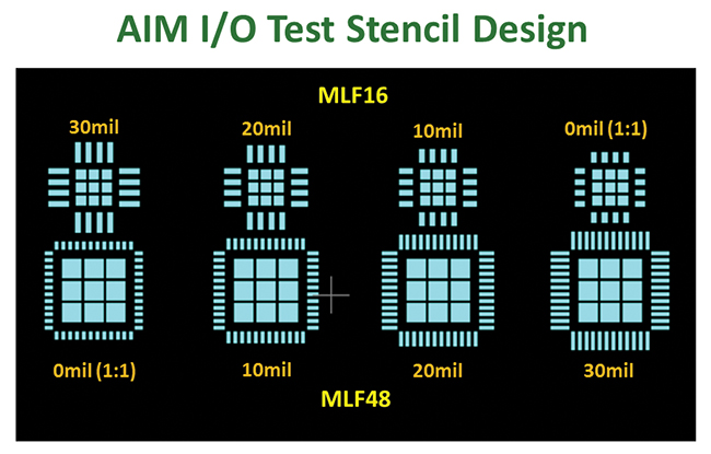
FIGURE 1. Test stencil design.
Figure 2 shows the effect of the overprinting on void formation on three different sizes of QFN: 16, 32 and 48 I/O. The drop in voiding is dramatic, and we were astonished at the results.
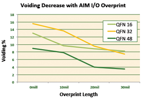
FIGURE 2. Voiding decrease with overprint increase.
Voids were consistently reduced by 1/3 or more simply by increasing the volume of solder paste on the I/O pads. The next obvious question is “what is causing these dramatic, repeatable voiding reductions?” Unfortunately, peering inside a convection oven during the reflow process to observe what’s happening, in real-time, on minute solder deposits is not possible. So we have examined the physical evidence and developed a theory on what improved the outgassing during the reflow process.
Our theory is depicted in Figure 3. We believe that, because the I/Os are on the perimeter, they reach liquidus temperature before the center pad. As they melt, the overprints coalesce onto the I/O pads, lifting the component for a very short period of time – the time between the outside melting and the inside melting. As soon as the print on centerpad melts and wets, the package collapses the solder. We think that momentarily lifting the lid formed by the component enables rapid outgassing and/or the collapse of the component itself forces gas out as it compresses the liquid solder underneath it.
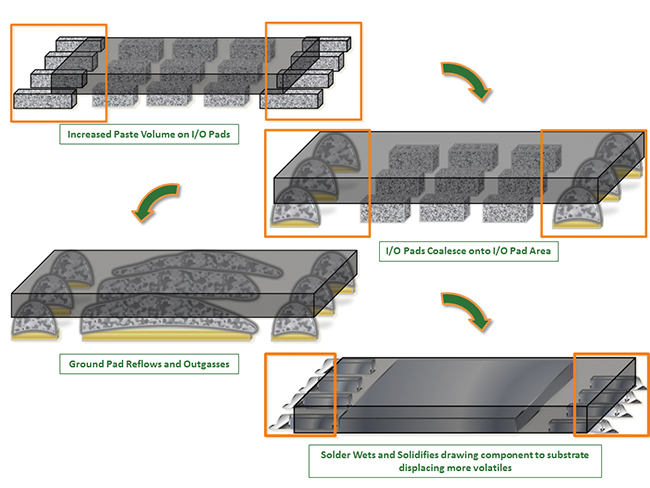
FIGURE 3. Theory of center pad void reduction.
In our experiments, the standoff height appeared to be set by the center pad. Different overprint lengths did not substantially affect standoff heights. The extra solder that was printed on the I/O pads migrated to the toes and is visible as darker areas on the X-rays. We created 5760 solder joints in this last run, and didn’t see any bridging or solder balling on any of the devices, even with the 30mil I/O overprint.
We deliberately didn’t do anything fancy on these tests. We used our standard test materials and set up, with a popular Type 4, no-clean SAC305 solder paste, printed with a 4mil (100μm) premium stainless steel stencil with a fluoropolymer nanocoating on our usual PCB2009 test board. A ramp-to-spike, or linear, profile was used. Most void reducing reflow profiles incorporate prolonged thermal exposure or soak zones to promote flux volatilization prior to the alloy reaching liquidus temperatures. The goal of this study was to isolate and assess the efficacy of the I/O paste overprint; therefore we used the least forgiving thermal profile.
The X-ray results were analyzed both visually and with statistical software. Figure 4 shows the pictures and the data for the 48 I/O QFN. Seeing is believing and the X-rays offer the most convincing visual evidence that this technique works and works well at void mitigation. The statistics quantify the impact of the I/O overprint on voiding rates, reinforcing the visual images with solid numbers.
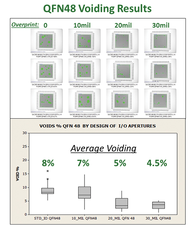
FIGURE 4. Images and statistical data for a 48-I/O QFN.
Armed with this compelling data, we are embarking on host of analyses and experiments. We are looking at mathematical relationships, theoretical height differentials, component masses, solid solder volumes, and ratios of pad areas, volumes and fillet lines. More areas to investigate come to mind almost every day. And we’re busy designing the next experiment:
- What will happen if we try a different paste?
- Will a water-soluble paste realize a similar result?
- Will a soak profile further reduce voiding? By how much?
- Will changing the solder paste volume on the ground pad further reduce the voiding? Can we now add more paste to the ground pad to achieve higher standoff?
- Can the I/O pad aperture design be further refined to provide more benefits?
- Can we tune in a “sweet spot?”
We are excited to continue evolving this technique, as it is currently in its infancy. We have a lot to learn about it, particularly in terms of design optimization.
So that’s it. No need for costly preforms or elaborate profiles or inert reflow atmospheres. Simply increasing the volume on the I/O pads may hold the key to one of the most effective and easy-to-use voiding remedies – one that provides a significant improvement to arguably the most common frustration on every SMT production floor around the world. And, best of all, IT’S FREE!
Written By Tim O’Neill, Technical Marketing Manager
Published in CIRCUITS ASSEMBLYDownload: ![]() AIM Tech Tip – Aperture Design to Minimize QFN Voiding
AIM Tech Tip – Aperture Design to Minimize QFN Voiding